- 您现在的位置:买卖IC网 > Sheet目录336 > KIT34716EPEVBE (Freescale Semiconductor)KIT EVAL BOARD 1MHZ DUAL SW-MODE
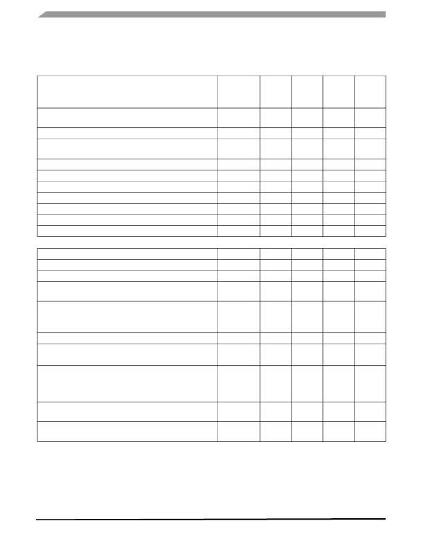
ELECTRICAL CHARACTERISTICS
STATIC ELECTRICAL CHARACTERISTICS
Table 3. Static Electrical Characteristics (continued)
Characteristics noted under conditions 3.0 V ? V IN ? 6.0 V, - 40 ? C ? T A ? 85 ? C, GND = 0 V, unless otherwise noted. Typical
values noted reflect the approximate parameter means at T A = 25°C under nominal conditions, unless otherwise noted.
Characteristic
Low Side N-CH Power MOSFET (M5) R DS(ON) (15)
Symbol
R DS(ON)LS1
Min
10
Typ
-
Max
50
Unit
m ?
(I OUT1 = 1.0 A, V IN = 3.3 V)
M2 R DS(ON)
R DS(ON)M2
2.0
-
4.0
?
(V IN = 3.3 V, M2 is on)
SW1 Leakage Current (Standby and Shutdown modes)
PVIN1 Pin Leakage Current
I SW
I PVIN1
-10
-10
-
-
10
10
μA
μA
(Shutdown Mode)
Error Amplifier DC Gain (15)
Error Amplifier Unit Gain Bandwidth (15)
Error Amplifier Slew Rate (15)
Error Amplifier Input Offset (15)
INV1 Pin Leakage Current
Thermal Shutdown Threshold (15)
Thermal Shutdown Hysteresis (15)
A EA
UGBW EA
SR EA
OFFSET EA
I INV1
T SDFET1
T SDHYFET1
-
-
-
-3.0
-1.0
-
-
150
3.0
7.0
0
-
170
25
-
-
-
3.0
1.0
-
-
dB
MHz
V/μs
mV
μA
°C
°C
CHANNEL 2 BUCK CONVERTER (PVIN2, SW2, PGND2, BOOT2, INV2, COMP2)
CH 2 High Side MOSFET Drain Voltage Range
P VIN
2.5
-
6.0
V
Output Voltage Adjustment
Range (15)
V OUTHI2
0.7
-
1.35
V
Output Voltage
Line Regulation
Accuracy (15) , (16),(17)
(15)
-
REG LN2
-1.0
-1.0
-
-
1.0
1.0
%
%
(Normal Operation, V IN = 3.0 to 6.0 V, I OUT2 = ±3.0 A)
Load Regulation (15)
REG LD2
-1.0
-
1.0
%
(Normal Operation, I OUT2 = -3.0 to 3.0 A)
Error Amplifier Common Mode Voltage Range (15),(18)
Output Under-voltage Threshold
Output Over-voltage Threshold
Continuous Output Current
Over-current Limit ?
(Sinking and Sourcing)
Short-circuit Current Limit ?
(Sinking and Sourcing)
High Side N-CH Power MOSFET (M6) R DS(ON) (15)
V REF2
V UVR2
V OVR2
I OUT2
I LIM2
I SHORT2
R DS(ON)HS2
0.0
-8.0
1.5
-3.0
-
-
10
-
-
-
-
4.0
6.5
-
1.35
-1.5
8.0
3.0
-
-
50
V
%
%
A
A
A
m ?
(I OUT2 = 1.0 A, V BOOT2 - V SW2 = 3.3 V)
Low Side N-CH Power MOSFET (M7) R DS(ON) (15)
R DS(ON)LS2
10
-
50
m ?
(I OUT2 = 1.0 A, V IN = 3.3 V)
Notes
15.
16.
17.
18.
Design information only, this parameter is not production tested.
Overall output accuracy is directly affected by the accuracy of the external feedback network, 1% feedback resistors are recommended
±1% is assured at room temperature
The 1% output voltage regulation is only guaranteed for a common mode voltage range greater than or equal to 0.7 V
34716
Analog Integrated Circuit Device Data ?
8
Freescale Semiconductor
发布紧急采购,3分钟左右您将得到回复。
相关PDF资料
KIT34717EPEVBE
KIT EVAL BOARD 5A 1.0MHZ
KS-1787-MG
SHELF SLIDING KEYBOARD ASSEMBLY
KS-1788
SHELF SLIDING KEYBOARD ASSEMBLY
KSDKSTM32-PL
KIT IAR KICKSTART STM32 CORTEXM3
LC4064ZC-EV
BOARD EVAL FOR ISPMACH 4064ZC
LCMXO2280C-C-EVN
BOARD CONTROL EVAL MACHXO
LDB100-024SW
LED POWER SUPPLY 24V 0-4A 100W
LDB150-048SW
LED POWER SUPPLY 24V-48V 3.125A
相关代理商/技术参数
KIT34717EPEVBE
功能描述:电源管理IC开发工具 5.0 A 1.0MHZ FULLY INTEG RoHS:否 制造商:Maxim Integrated 产品:Evaluation Kits 类型:Battery Management 工具用于评估:MAX17710GB 输入电压: 输出电压:1.8 V
KIT34727FCEVBE
功能描述:电源管理IC开发工具 600MA HIGH EFFICIENCY LO RoHS:否 制造商:Maxim Integrated 产品:Evaluation Kits 类型:Battery Management 工具用于评估:MAX17710GB 输入电压: 输出电压:1.8 V
KIT34825EPEVME
功能描述:界面开发工具 MICRO USB INTERFACE IC RoHS:否 制造商:Bourns 产品:Evaluation Boards 类型:RS-485 工具用于评估:ADM3485E 接口类型:RS-485 工作电源电压:3.3 V
KIT34844AEPEVBE
功能描述:LED 照明开发工具 IC, 10 CHANNEL LED BACKLIGHT RoHS:否 制造商:Fairchild Semiconductor 产品:Evaluation Kits 用于:FL7732 核心: 电源电压:120V 系列: 封装:
KIT34844EPEVME
功能描述:LED 照明开发工具 MC34844 10-Ch LED BL Driver Eval Kit
RoHS:否 制造商:Fairchild Semiconductor 产品:Evaluation Kits 用于:FL7732 核心: 电源电压:120V 系列: 封装:
KIT34845EPEVME
功能描述:LED 照明开发工具 IC, 6 CHANNEL LED BACKL RoHS:否 制造商:Fairchild Semiconductor 产品:Evaluation Kits 用于:FL7732 核心: 电源电压:120V 系列: 封装:
KIT34929EPEVME
功能描述:电源管理IC开发工具 1.0 A/ 28 V BRUSHLESS DC
RoHS:否 制造商:Maxim Integrated 产品:Evaluation Kits 类型:Battery Management 工具用于评估:MAX17710GB 输入电压: 输出电压:1.8 V
KIT3500UZ
功能描述:KIT CAP CERM HI FREQ 1210 RoHS:是 类别:套件 >> 无源 - 电容器 系列:U 标准包装:1 系列:SP-Cap CD, CX, SL, SX 套件类型:聚合物,铝电解 值:135 件 - 39µF ~ 470µF,各 15 件 包装:- 安装类型:表面贴装 包括封装:7343-17,7343-20 产品目录页面:2651 (CN2011-ZH PDF) 工具箱内容:(15) PCE4991CT-ND - CAP ALUM 220UF 4V 20% SMD(15) PCE4990CT-ND - CAP ALUM 330UF 2V 20% SMD(15) PCE4989CT-ND - CAP ALUM 150UF 6.3V 20% SMD(15) PCE4988CT-ND - CAP ALUM 150UF 6.3V 20% SMD(15) PCE4943CT-ND - CAP ALUM 39UF 10V 20% SMD(15) PCE4823CT-ND - CAP ALUM 470UF 2V 20% SMD(15) PCE4816CT-ND - CAP ALUM 220UF 4V 20% SMD(15) PCE4479CT-ND - CAP ALUM 220UF 2V 20% SMD(15) PCE4472CT-ND - CAP ALUM 120UF 2V 20% SMD 其它名称:SP4-KIT
